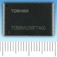
 Toshiba Corporation today announced the development of BENAND, a versatile, multi-application single level cell (SLC) NAND flash memory with an embedded error correction code (ECC). BENAND's diverse applications include LCD TVs and digital cameras along with robots and other industrial applications. Samples of eight BENAND products in two capacities, 4Gigabit and 8Gigabit, will be available from today and mass production will follow from March 2012.
The simple interface and high reliability of small capacity SLC NAND has won it wide use in consumer applications and industrial programming. Until now, the ECC has been embedded in the host processor and corrected 1 bit per 512 bytes. However, advances in memory process technology require enhanced error correction; more than 4 bit correction per 512 bytes for NAND flash fabricated with 32nm process. For NAND flash memory without ECC fabricated with 32nm and beyond, the controller in the host processor must be changed to secure the required level of correction.
BENAND removes the burden of ECC from the host processor while minimizing protocol changes and allowing host processors to support leading-edge process NAND flash memory in a timely manner. BENAND embeds an ECC with an error correction of 4 bit per 512 bytes onto Toshiba's cutting-edge 32nm process SLC NAND flash memory. Package and pin configuration compatibility are assured with general SLC NAND flash, allowing easy replacement of existing products.
Toshiba plans to expand the BENAND lineup to include 24nm process NAND flash memory products after summer 2012. Adding SLC embedded NAND flash memory expands the company's line-ups and offers customers more choices, and will support Toshiba's advances in memory business.
Main Features
- 4 bit per 512 bytes ECC and 32nm process NAND flash memory are embedded in one package.
- Embedded a versatile interface. Package and pin configuration compatibility are ensured with general SLC NAND flash, allowing easy replacement of existing products.
- Allows the host processor to apply cutting-edge process NAND flash memory regardless of the error correction ability of the host processor by embedding ECC in the NAND flash memory itself.
Specifications
- Interface - General NAND flash memory interface
- Page Size - 4K Byte
- Voltage - Vcc=2.7~3.6V, 1.7~1.95V
- Package
- 48 pin TSOP (12mm x 20mm x 1.2mm)
- 63 ball FBGA (9mm x 11mm x 1.0mm)

